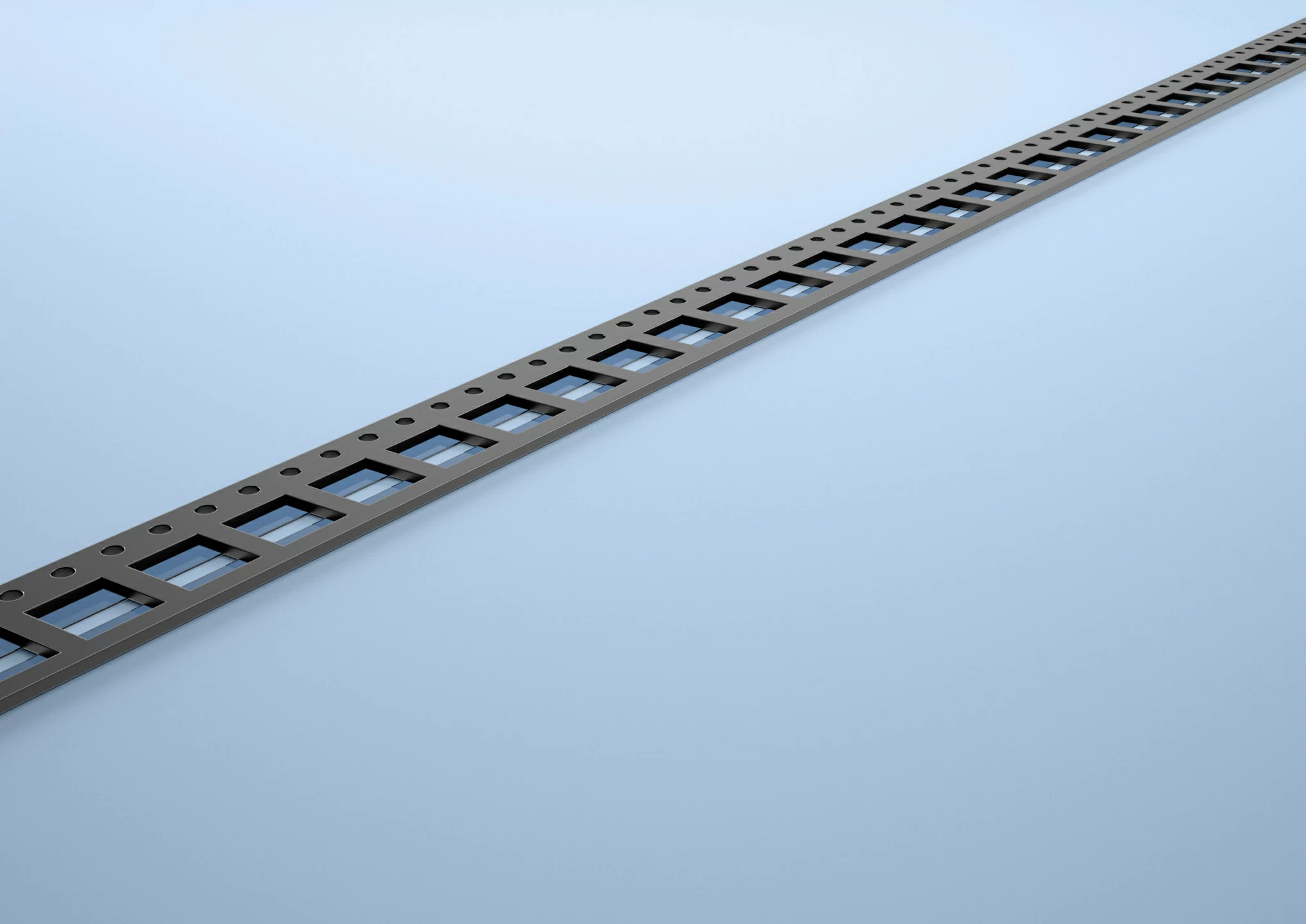
Advantek's unique form of punched carrier tape - ideal for bare die or small devices where protection and placement are critical.
Components are placed on a wafer film backing within a compartment boundary. Unlike conventional embossed tape, the compartment does not have to be sized to the component, eliminating the need for custom carrier tape tooling. Traditional cover tape is also not required. Both elements reduce inventory management costs.
Surftape is also an excellent solution for shipping prototypes or early production runs. Surf tape comes in standard sizes—no need to wait for tape design and custom tooling.
- Ideal for bare die, chip-scale packages, MEMs, LEDs, and micro-thin components, Surftape ensures devices are securely held in place - preventing corners, edges, and surfaces from contacting the packing material, and maintaining component integrity.
- Devices are secured in the exact position they are placed, eliminating the need for theta correction during automated assembly.
- One tape size can accommodate multiple component sizes, reducing tooling costs and eliminating large minimum order requirements.
- Supporting EIA 747 - semiconductor industry packaging standard.
Material Properties
| Property | Typical value | Test Method |
| Specific Gravity | 1.12 g/cc | ISO 1183 |
| Tensile Strength | 29 Mpa | ISO 527 |
| Tensile Elongation | 40% | ISO 527 |
| Flexural Strength | 46 Mpa | ISO 178 |
| Heat Distortion | 85°C | ASTM D1525 |
| Surface Resistivity | ≥104, <108 Ohms/Sq | ASTM D257 |
| Carrier Tape Thickness | 0.64 & 0.84 mm | EN 1942 |
| Adhesive Tape Thickness | 0.075 mm | EN 1942 |
| Total Thickness | 0.724 & 0.924 mm | EN 1942 |